คําอธิบายสินค้า:
การประชุม PCB การสื่อสารเป็นแผ่นวงจรพิมพ์ที่มีความเชี่ยวชาญสูงที่ออกแบบเพื่อตอบสนองความต้องการที่เข้มงวดของระบบสื่อสาร 5G ใหม่ด้วยการพัฒนาเทคโนโลยีโทรคมนาคมอย่างรวดเร็ว, ความต้องการของทางแก้ไข PCB ที่แข็งแกร่ง, น่าเชื่อถือและมีประสิทธิภาพสูงไม่เคยมากกว่านี้.,การรับรองการส่งข้อมูลอย่างต่อเนื่อง และการเพิ่มความสมบูรณ์ของสัญญาณ
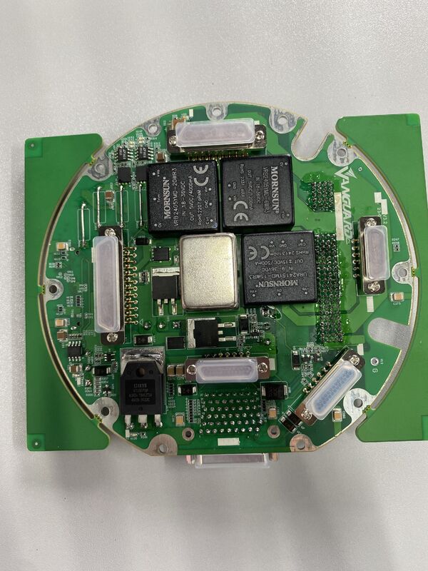
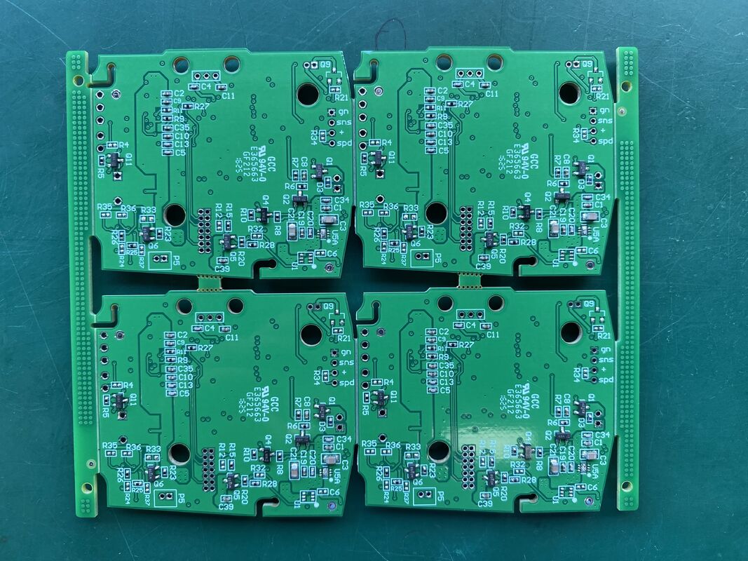
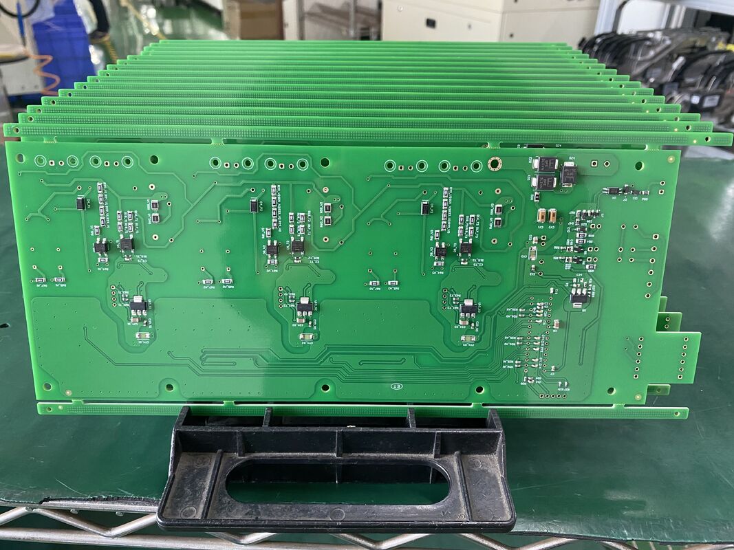
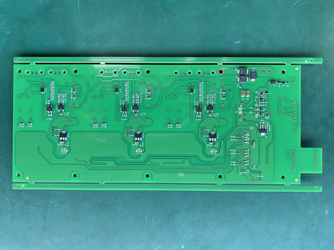
หนึ่งในลักษณะที่โดดเด่นของงานประกอบ PCB การสื่อสารนี้ คือขนาดที่สามารถปรับแต่งได้ โดยทําให้สามารถหาคําตอบที่เหมาะสมกับความต้องการของอุปกรณ์ได้อย่างสมบูรณ์แบบไม่ว่าการใช้งานของคุณจะต้องการ PCB compact หรือบอร์ดขนาดใหญ่, ผลิตภัณฑ์นี้สามารถผลิตได้อย่างแม่นยําเพื่อตอบสนองความต้องการพิเศษของคุณ ความหนาของแผ่นยังสามารถปรับแต่งได้, ตั้งแต่ 0.2 มิลลิเมตรถึง 6 มิลลิเมตร, ให้ความยืดหยุ่นในการออกแบบและความแข็งแรงทางกลความสามารถในการปรับปรุงนี้มีความสําคัญสําหรับอุปกรณ์การสื่อสารต่างๆ, ที่มีข้อจํากัดพื้นที่และความทนทานเป็นข้อพิจารณาสําคัญ
กว้างขวางรูขนาดเล็ก 0.1 มิลลิเมตร ชี้ให้เห็นถึงความสามารถในการผลิตความละเอียดของชุด PCB นี้ การเจาะละเอียดเช่นนี้ทําให้การบูรณาการขององค์ประกอบความหนาแน่นสูงซึ่งเป็นสิ่งจําเป็นในอุปกรณ์สื่อสาร 5G ที่ต้องการการลดขนาดเล็ก โดยไม่เสียผลงานช่องทางและหลุมเล็ก ๆ เหล่านี้อํานวยความสะดวกในการเชื่อมต่อไฟฟ้าที่มีประสิทธิภาพและการนําสัญญาณไปส่ง ส่งผลต่อประสิทธิภาพและความน่าเชื่อถือของระบบสื่อสาร
การรวมการป้องกันการกระชับกระชับกระชับกระชับกระชับกระชับกระชับกระชับกระชับกระชับกระชับกระชับกระชับกระชับกระชับความเปลี่ยนแปลงของพลังงาน, หรือเหตุการณ์ชั่วคราวอื่น ๆ ชุด PCB นี้ถูกออกแบบมาเพื่อบูรณาการองค์ประกอบป้องกันการกระชับกระแสที่ป้องกันวงจรอิเล็กทรอนิกส์ที่มีความรู้สึกจากความเสียหายด้วยการลดความเสี่ยงของการกระแทกไฟฟ้า, การประกอบการเพิ่มอายุยาวและความมั่นคงของอุปกรณ์การสื่อสาร, รับประกันการบริการที่ไม่หยุดยั้งและลดเวลาหยุดทํางานให้น้อยที่สุด.
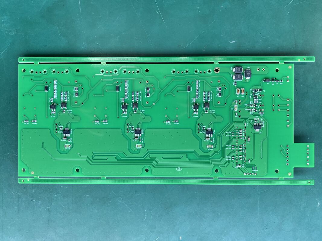
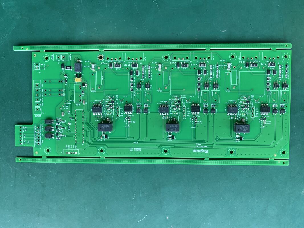
คุณสมบัติที่สําคัญอีกอย่างของสินค้านี้ คือความสามารถในการจัดการกับภาระไฟฟ้าที่แรงองค์ประกอบของพื้นฐานการสื่อสารมักต้องการการส่งกระแสไฟฟ้าที่สําคัญ เพื่อให้พลังงานให้กับโมดูลต่าง ๆ และรักษาความแข็งแรงของสัญญาณการประกอบ PCB การสื่อสารถูกออกแบบเพื่อรองรับการใช้งานกระแสไฟฟ้าที่หนัก มีรอยทองแดงที่แข็งแรงและการจัดการความร้อนที่ปรับปรุงนี่ทําให้แน่ใจว่า PCB สามารถทํางานอย่างปลอดภัยและมีประสิทธิภาพภายใต้สภาพไฟฟ้าที่ต้องการ, ป้องกันการอุ่นเกินและรักษาความสมบูรณ์ของสัญญาณ
ด้านการปรับแต่งของประกอบการ PCB สื่อสารนี้ยืดกว้างไปกว่าขนาดและความหนา ลูกค้าสามารถกําหนดปริมาตรต่าง ๆ ให้เหมาะสมกับความต้องการการใช้งานเฉพาะเจาะจงของพวกเขารวมถึงการเลือกวัสดุระดับการปรับเปลี่ยนนี้ทําให้แน่ใจว่าทุก PCB แอนกบิ้ลจะสอดคล้องอย่างสมบูรณ์แบบกับความต้องการทางการทํางานและสิ่งแวดล้อมของอุปกรณ์การสื่อสาร 5Gไม่ว่าจะใช้ในสถานีฐาน, แอนเทนน์ หรือองค์ประกอบสําคัญอื่นๆ ของพื้นฐานการสื่อสาร
สรุปคือ การประกอบ PCB การสื่อสาร เป็นทางออกที่ทันสมัยและสามารถปรับปรุงได้ สําหรับภูมิทัศน์การสื่อสาร 5G ที่กําลังพัฒนาความหนาของแผ่นยืดหยุ่นตั้งแต่ 0.2mm ถึง 6mm และความสามารถในการรองรับการใช้งานกระแสไฟฟ้าที่แรงทําให้มันเป็นตัวเลือกที่เหมาะสมสําหรับพื้นฐานการสื่อสารที่ทันสมัยการป้องกันส่วนประกอบอิเล็กทรอนิกส์ที่สําคัญจากอันตรายทางไฟฟ้าโดยการนําเสนอการออกแบบที่สามารถปรับแต่งได้อย่างเต็มที่ชุด PCB นี้ทําให้วิศวกรและผู้ผลิตสามารถสร้างอุปกรณ์สื่อสารที่ทันสมัย ที่ตอบสนองมาตรฐานคุณภาพและการทํางานที่สูงสุด.
ไม่ว่าคุณจะปรับปรุงระบบสื่อสารที่มีอยู่ หรือพัฒนาเทคโนโลยี 5G ใหม่ สัมมนา PCB การสื่อสารนี้และทางแก้ไขการสื่อสารที่ทนทานคุณสมบัติที่ทันสมัยและความสามารถในการปรับปรุงมันทําให้มันสามารถตอบโจทย์กับสิ่งท้าทายของสภาพแวดล้อมการสื่อสารที่วิ่งเร็วในปัจจุบัน ทําให้มันเป็นองค์ประกอบที่จําเป็นในด้านโทรคมนาคม
ลักษณะ:
- ชื่อสินค้า: การสื่อสาร PCB Assembly
- ปลายผิว: ENIG, HASL ไม่มีหมูเพื่อเพิ่มความทนทานและความสามารถในการนําไฟ
- กว้างขวางรูขั้นต่ํา: 0.1mm สําหรับการวางส่วนประกอบอย่างแม่นยํา
- ชั้น PCB: 6 ชั้นเพื่อรองรับการออกแบบวงจรที่ซับซ้อน
- รายละเอียด: PCB ขนาดที่กําหนดตามความต้องการโครงการ
- สาขาใช้งาน: การสื่อสาร 5G เหมาะสมสําหรับพื้นฐานการสื่อสารที่ทันสมัย
- รวมถึงคุณสมบัติการป้องกันการกระชับกระชับกระชับกระแสเพื่อให้มีความน่าเชื่อถือภายใต้สปิกความดัน
- รวมชั้นทองแดงหนาสําหรับการปรับปรุงความสามารถในการบรรทุกกระแสไฟฟ้าและการจัดการความร้อน
ปริมาตรเทคนิค:
| ชั้น PCB |
6 ชั้น |
| กว้างของหลุม |
0.1 มม. |
| ประเภทชีวิต |
ผ่านหลุม ตาบอด ถูกฝัง |
| การบํารุงผิว |
ENIG, HASL ไม่มีหมู |
| กล่องภายนอก |
กล่อง |
| ปรับแต่ง |
ใช่ |
| ระบบคุณภาพ PCB |
ROHS |
| การสื่อสาร PCB |
Tgสูง 170 และ Tgสูง 180 |
| ความหนาของแผ่น |
0.2-6 มิลลิเมตร |
| รายละเอียด |
ขนาด PCB ที่กําหนดเอง |
การใช้งาน:
การสื่อสาร PCB Assembly มีบทบาทสําคัญในพื้นฐานการสื่อสารที่ทันสมัย โดยให้ความมั่นใจในการส่งข้อมูลที่น่าเชื่อถือและมีประสิทธิภาพออกแบบด้วยความหนาของแผ่นตั้งแต่ 0.2mm ถึง 6mm สินค้านี้มีความหลากหลาย เหมาะสําหรับอุปกรณ์การสื่อสารและอุปกรณ์ต่างๆขนาด PCB ที่สามารถปรับเปลี่ยนได้ ทําให้ผู้ผลิตสามารถปรับแต่งชุดได้อย่างแม่นยําตามความต้องการของโครงการการประกันผลงานที่ดีที่สุดและการบูรณาการอย่างต่อเนื่อง ภายในระบบสื่อสารที่ซับซ้อน
หนึ่งในโอกาสการใช้งานหลักสําหรับการประกอบ PCB สื่อสารคือการพัฒนาและบํารุงรักษาโครงสร้างพื้นฐานการสื่อสาร รวมถึงรูเตอร์, สวิตช์, สถานีฐานและหน่วยประมวลผลสัญญาณความสามารถในการปรับเปลี่ยนสีหน้ากากผสม เช่น สีฟ้าหรือสีเขียวทําให้ผู้ผลิตสามารถตอบสนองความต้องการทางด้านความสวยงามและการทํางานเฉพาะอย่างยิ่ง โดยปรับปรุงความทนทานและการป้องกันของแผ่นวงจรความใส่ใจในรายละเอียดนี้ทําให้การประกอบสามารถทนต่อความท้าทายทางสิ่งแวดล้อมและรักษาการทํางานที่มั่นคงตลอดระยะเวลานาน
ในฉากที่เกี่ยวข้องกับการใช้งานกระแสไฟฟ้าที่แรง การประกอบ PCB การสื่อสารได้รับการออกแบบเพื่อจัดการกับภาระไฟฟ้าเพิ่มขึ้นอย่างปลอดภัยและมีประสิทธิภาพ1mm รองรับส่วนประกอบความละเอียดและการวางแผนวงจรความหนาแน่นสูง, ซึ่งเป็นสิ่งสําคัญสําหรับอุปกรณ์การสื่อสารที่ทันสมัยที่ต้องการความคอมแพคต์และความแม่นยําและโครงสร้างเครือข่ายพึ่งพาการประกอบเหล่านี้เพื่อให้ผลงานสูงในสภาพการทํางานที่ต้องการ.
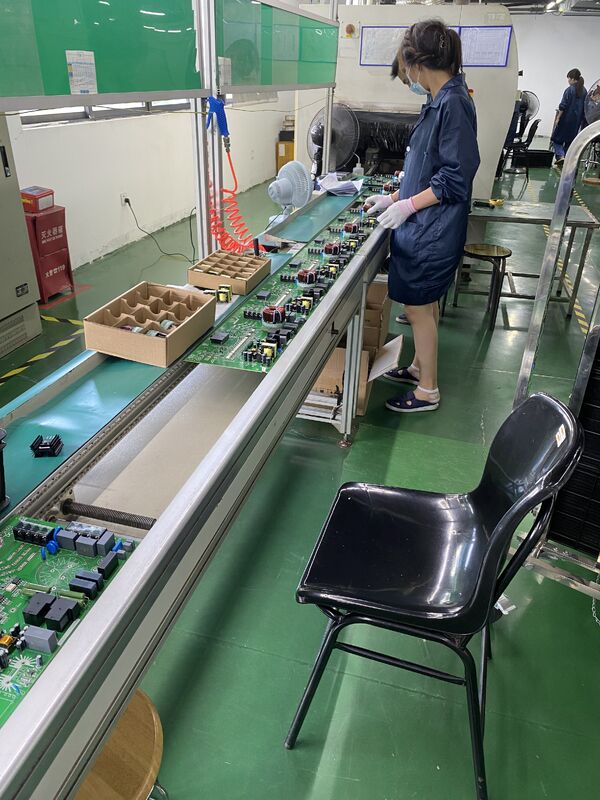
การบรรจุภายนอกในกระดาษกล่องที่ทนทานทําให้ประกอบ PCB การสื่อสารถึงสถานที่ผลิตหรือสถานที่ติดตั้งในสภาพเดิม โดยไม่เสียหายระหว่างการขนส่งการ แพ็ค แพ็ค กล่อง อย่าง ระมัดระวัง นี้ เป็น สิ่ง สําคัญ สําหรับ การ รักษา ความ ซื่อ สัตย์ ของ องค์ประกอบ อิเล็กทรอนิกส์ ที่ อ่อนโยน และ การ รับประกัน กระบวนการ ผลิต ที่ เรียบร้อยไม่ว่าจะเป็นการใช้ในโครงการพื้นฐานขนาดใหญ่ หรืออุปกรณ์สื่อสารขนาดเล็กรวมเหล่านี้ให้บริการทางแก้ไขที่น่าเชื่อถือที่สนับสนุนการพัฒนาต่อเนื่องของเทคโนโลยีการสื่อสาร.
โดยสรุป การประกอบ PCB การสื่อสารเป็นสิ่งจําเป็นสําหรับผู้ผลิตที่เน้นการพัฒนาพื้นฐานการสื่อสารการออกแบบที่แข็งแกร่งสําหรับการใช้งานไฟฟ้าแรง, และความใส่ใจในรายละเอียดการบรรจุทําให้มันเป็นตัวเลือกที่เหมาะสมสําหรับฉากการสื่อสารที่หลากหลาย, รับประกันความน่าเชื่อถือ, ประสิทธิภาพและอายุยืนในระบบอิเล็กทรอนิกส์ที่สําคัญ.
การปรับแต่ง:
ผลิตภัณฑ์การประกอบ PCB สื่อสารของเรานําเสนอบริการการปรับแต่งที่ครบวงจรที่ปรับแต่งเพื่อตอบสนองความต้องการเฉพาะเจาะจงของอุตสาหกรรมสื่อสาร 5Gเรารับประกันความแม่นยําและความน่าเชื่อถือในทุกกระดานเราเชี่ยวชาญในการผลิต PCB การสื่อสารที่มีวัสดุ Tg170 และ Tg180 สูง, ให้ความมั่นคงทางความร้อนที่ดีเยี่ยมสําหรับการใช้งานที่ต้องการ.
PCBs ของเราถูกออกแบบมาเพื่อพื้นฐานการสื่อสาร เพื่อรองรับแรงกระแสไฟฟ้าที่หนัก และมีชั้นทองแดงหนา เพื่อเพิ่มความสามารถในการนําไฟและความทนทานเรานําเสนอขนาด PCB ที่กําหนดเองให้เหมาะสมกับความต้องการโครงการพิเศษของคุณ, รับประกันผลงานที่ดีที่สุดในระบบสื่อสาร 5G ที่ทันสมัย
เลือกบริการประกอบ PCB สื่อสารที่กําหนดเองของเรา เพื่อได้รับประโยชน์จากคําตอบที่มีคุณภาพสูง, น่าเชื่อถือ และมีประสิทธิภาพที่ตอบสนองมาตรฐานที่เข้มงวดของเทคโนโลยีสื่อสารที่ทันสมัย
การสนับสนุนและบริการ:
ผลิตภัณฑ์การประกอบ PCB การสื่อสารของเราได้รับการสนับสนุนจากทีมงานสนับสนุนทางเทคนิคที่มอบความช่วยเหลือครบวงจรตลอดรอบชีวิตของสินค้าเราให้คําแนะนําเชี่ยวชาญในการติดตั้ง, การตั้งค่า และการแก้ไขปัญหา เพื่อให้การทํางานและความน่าเชื่อถือที่ดีที่สุด
บริการรวมถึงการให้คําปรึกษาอย่างละเอียดเกี่ยวกับการออกแบบเพื่อการผลิต โปรต็อกอลการทดสอบที่เข้มงวด และการอัพเดทฟอร์มแวร์ เพื่อให้ระบบสื่อสารของคุณทํางานได้อย่างเรียบร้อยทีมงานของเรามีอุปกรณ์ที่เหมาะสมในการจัดการกับความต้องการที่กําหนดเอง และให้คําตอบที่เหมาะสมเพื่อตอบสนองความต้องการการใช้งานเฉพาะเจาะจงของคุณ.
นอกจากนี้ เรายังให้บริการด้านการบํารุงรักษา รวมถึงการวินิจฉัยและซ่อมแซม เพื่อลดเวลาหยุดทํางานให้น้อยที่สุด และขยายอายุการใช้งานของ PCB ของคุณมีประสิทธิภาพ, และการสนับสนุนทางมืออาชีพเพื่อช่วยให้คุณบรรลุการบูรณาการในพื้นฐานการสื่อสารได้อย่างต่อเนื่อง
การบรรจุและการขนส่ง
ผลิตภัณฑ์ประกอบ PCB การสื่อสารของเราถูกบรรจุอย่างรอบคอบ เพื่อให้ความคุ้มกันสูงสุดระหว่างการขนส่งตามด้วยวัสดุการบรรจุที่อุดหนุนเพื่อดูดซึมกระแทกและสั่นสะเทือน.
จากนั้นการประกอบก็ถูกบรรจุไว้ในกล่องที่แข็งแรง เพื่อทนต่อสภาพการใช้งานและการส่งเรายังรวมถุงป้องกันความชื้นและ desiccants เมื่อจําเป็นต้องป้องกันจากความชื้น.
สําหรับการจัดส่ง เราร่วมมือกับผู้ขนส่งที่น่าเชื่อถือ เพื่อให้มีการจัดส่งที่ทันเวลาและปลอดภัยทั่วโลกข้อมูลการติดตามถูกจัดให้บริการสําหรับทุกการจัดส่ง เพื่อให้ลูกค้าของเราทราบตลอดกระบวนการจัดส่ง.
การขอบรรจุอาหารพิเศษสามารถตอบสนองได้ตามคําถามของลูกค้า เพื่อตอบสนองความต้องการหรือมาตรฐานความสอดคล้องที่พิเศษ


 ข้อความของคุณจะต้องอยู่ระหว่าง 20-3,000 ตัวอักษร!